| CPC H01L 29/7781 (2013.01) [H01L 29/407 (2013.01); H01L 29/435 (2013.01); H01L 29/4916 (2013.01); H01L 29/4983 (2013.01); H01L 29/66431 (2013.01)] | 17 Claims |

|
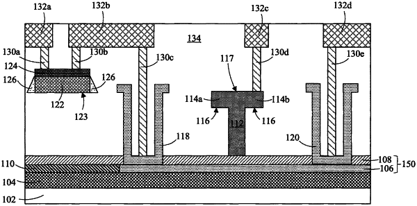
1. A semiconductor device comprising:
an active region above a substrate, the active region comprising a channel layer and a barrier layer disposed on the channel layer;
source and drain electrodes in contact with the active region;
a gate above the active region, the gate is laterally between the source and drain electrodes, the gate has an upper surface;
a polysilicon layer above the substrate, the polysilicon layer has a lower surface, wherein the polysilicon layer is positioned laterally adjacent to the gate and the lower surface of the polysilicon layer is at a lower elevation than the upper surface of the gate;
a silicide layer on the polysilicon layer; and
an isolation layer above the substrate, the isolation layer being adjacent to the channel layer, wherein the polysilicon layer is positioned above the isolation layer.
|