| CPC H01L 29/402 (2013.01) [H01L 29/0649 (2013.01); H01L 29/2003 (2013.01); H01L 29/205 (2013.01); H01L 29/404 (2013.01); H01L 29/66462 (2013.01); H01L 29/78 (2013.01)] | 17 Claims |

|
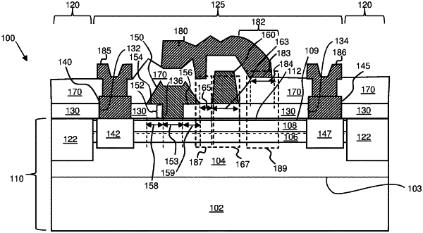
1. A semiconductor device comprising:
a semiconductor substrate that includes an upper surface and a channel;
a first dielectric layer disposed over the upper surface of the semiconductor substrate;
a first current-carrying electrode and a second current-carrying electrode formed over the semiconductor substrate within openings formed in the first dielectric layer, wherein the first current-carrying electrode and the second current-carrying electrode are electrically coupled to the channel;
a control electrode formed over the semiconductor substrate and disposed between the first current-carrying electrode and the second current-carrying electrode and over the first dielectric layer, wherein the control electrode is electrically coupled to the channel;
a first conductive element formed over the first dielectric layer, electrically insulated from and adjacent to the control electrode, formed between the control electrode and the second current-carrying electrode;
a second dielectric layer disposed over the control electrode and over the first conductive element; and
a second conductive element disposed over the second dielectric layer and over the first conductive element, wherein a portion of the second conductive element is below an upper surface of the first conductive element between the control electrode and the first conductive element.
|