| CPC H01L 29/165 (2013.01) [H01L 21/823431 (2013.01); H01L 27/0886 (2013.01); H01L 29/0649 (2013.01)] | 3 Claims |

|
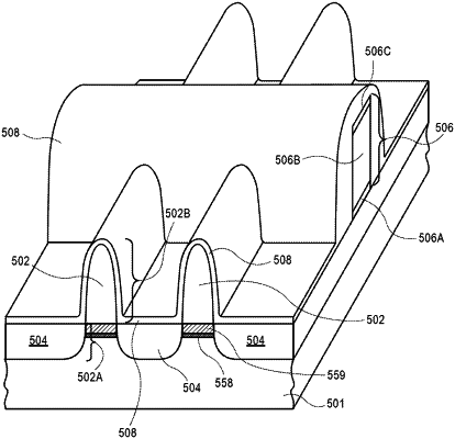
1. A method of fabricating an integrated circuit structure, the method comprising:
forming a trench in an isolation structure on a silicon substrate, the trench exposing a portion of the silicon substrate;
forming a lower silicon portion of a fin in the trench and on the exposed portion of the silicon;
forming an intermediate germanium portion of the fin in the trench and on the lower silicon portion of the fin;
forming a silicon germanium portion of the fin in the trench and on the intermediate germanium portion of the fin, wherein the intermediate germanium portion has a greater atomic concentration of germanium than the upper silicon germanium portion;
recessing the isolation structure to expose sidewalls of a portion of the fin; and
forming a gate stack on and along the exposed sidewalls of the portion of the fin.
|