| CPC H01L 29/0653 (2013.01) [H01L 29/0673 (2013.01); H01L 29/42392 (2013.01); H01L 29/66545 (2013.01); H01L 29/66818 (2013.01); H01L 29/7848 (2013.01); H01L 29/7854 (2013.01)] | 20 Claims |

|
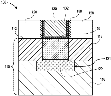
1. A method of forming a transistor, comprising:
forming a fin and a dummy gate over a substrate, wherein the fin comprises:
a sub-fin layer;
a source region over the sub-fin layer;
a drain region over the sub-fin layer;
a channel region over the sub-fin layer, wherein the channel region is between the source region and the drain region; and
wherein the dummy gate comprises:
a first spacer over the fin proximate to an interface between the source region and the channel region;
a second spacer over the fin proximate to an interface between the drain region and the channel region; and
a dummy gate electrode between the first spacer and the second spacer;
exposing the channel region by removing the dummy gate electrode;
selectively etching the sub-fin layer below the channel region to form a cavity;
disposing an insulating material in the cavity;
disposing a gate dielectric over the channel region; and
disposing a gate electrode over the gate dielectric.
|