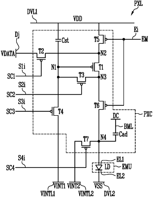
| CPC H01L 27/1255 (2013.01) [G09G 3/3233 (2013.01); H01L 25/167 (2013.01); G09G 2300/0426 (2013.01); G09G 2300/0819 (2013.01); G09G 2300/0852 (2013.01); G09G 2300/0861 (2013.01); G09G 2310/0278 (2013.01)] | 21 Claims |

|
1. A display device comprising:
a first conductive layer disposed on a substrate, and including an auxiliary bottom line and an additional conductive pattern;
a first insulating layer disposed on the substrate and the first conductive layer;
a semiconductor pattern disposed on the first insulating layer;
a second insulating layer disposed on the first insulating layer and the semiconductor pattern;
a second conductive layer disposed on the second insulating layer, and including a conductive pattern and a gate electrode spaced apart from each other;
a third insulating layer disposed on the second insulating layer and the second conductive layer;
a connection pattern disposed on the third insulating layer and electrically connected to the conductive pattern through a contact hole passing through the third insulating layer;
a first electrode disposed on the connection pattern and electrically connected to the connection pattern; and
at least one light emitting element disposed on the first electrode and electrically connected to the first electrode.
|