| CPC H01L 27/1207 (2013.01) [G11C 17/16 (2013.01); G11C 17/165 (2013.01); H01L 23/5252 (2013.01); H10B 20/20 (2023.02); H10B 20/25 (2023.02)] | 18 Claims |

|
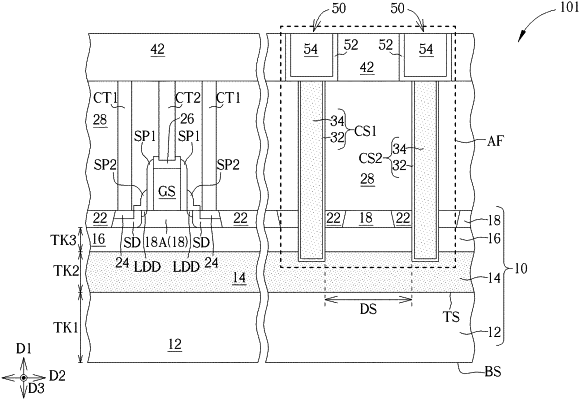
1. A semiconductor structure, comprising:
a semiconductor on insulator (SOI) substrate comprising:
a base substrate;
a buried insulation layer disposed on the base substrate;
a semiconductor layer disposed on the buried insulation layer; and
a trap rich layer disposed between the buried insulation layer and the base substrate;
a first electrically conductive structure, wherein at least a part of the first electrically conductive structure is disposed in the trap rich layer; and
a second electrically conductive structure, wherein at least a part of the second electrically conductive structure is disposed in the trap rich layer, a part of the trap rich layer is disposed between the first electrically conductive structure and the second electrically conductive structure, and the first electrically conductive structure, the second electrically conductive structure, and the trap rich layer disposed between the first electrically conductive structure and the second electrically conductive structure are at least a portion of an anti-fuse structure,
wherein the first electrically conductive structure and the second electrically conductive structure penetrate through the trap rich layer in a vertical direction, respectively.
|