| CPC H01L 27/1207 (2013.01) [G05F 1/56 (2013.01); G06F 1/26 (2013.01); H01L 21/0214 (2013.01); H01L 21/02164 (2013.01); H01L 21/0217 (2013.01); H01L 21/02178 (2013.01); H01L 21/02181 (2013.01); H01L 21/02183 (2013.01); H01L 21/02186 (2013.01); H01L 21/02192 (2013.01); H01L 21/02565 (2013.01); H01L 21/383 (2013.01); H01L 27/1225 (2013.01); H01L 29/24 (2013.01); H01L 29/42384 (2013.01); H01L 29/4908 (2013.01); H01L 29/66969 (2013.01); H01L 29/7869 (2013.01); H01L 29/78696 (2013.01); H01L 2029/42388 (2013.01)] | 8 Claims |

|
1. A voltage regulator comprising:
an input node to receive an input voltage;
an output node;
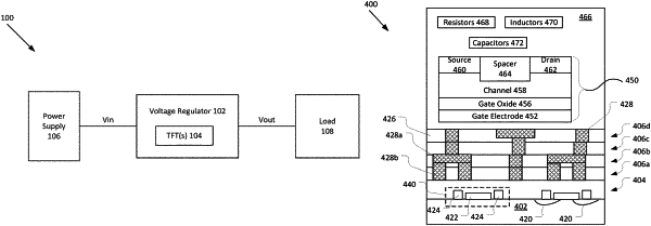
a voltage regulator circuit to receive the input voltage at the input node and generate a regulated output voltage at the output node, wherein the voltage regulator circuit includes a thin-film transistor (TFT);
wherein the TFT includes a channel layer that includes an oxide semiconductor material, wherein the channel layer includes a dopant; and
wherein the dopant includes a concentration gradient within the channel layer, wherein a higher concentration of the dopant is at a side of the channel layer proximate to a source or a drain of the TFT, and wherein an entirety of a bottom of the channel layer is in a same plane, and wherein the channel layer is a back end of line channel layer, wherein the TFT is over one or more back end of line interconnect layers, and wherein the one or more interconnect layers are over a front-end transistor.
|