| CPC H01L 27/098 (2013.01) [H01L 21/8232 (2013.01); H01L 21/823418 (2013.01); H01L 21/823493 (2013.01); H01L 27/088 (2013.01)] | 10 Claims |

|
1. A semiconductor device, comprising:
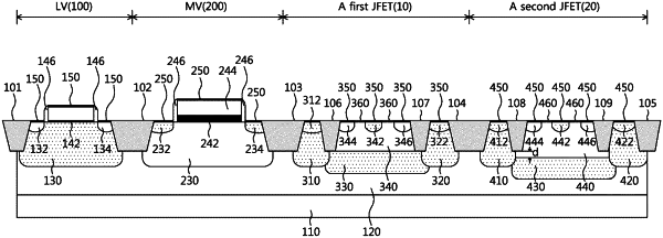
a first junction-gate field-effect transistor (JFET) having a first pinch-off voltage, the first JFET comprising:
a first top gate region disposed on a surface of a substrate;
a first channel region surrounding the first top gate region; and
a first bottom gate region disposed under the first channel region, wherein the first channel region and the first bottom gate region have different conductivity types from each other; and
a second JFET having a second pinch-off voltage higher than the first pinch-off voltage, comprising:
a second top gate region disposed on the surface and having a depth that is the same as a depth of the first top gate region relative to the surface;
a second channel region surrounding the second top gate region and having a depth that is greater than a depth of the first channel region relative to the surface; and
a second bottom gate region disposed under the second channel region and having a depth which is greater than a depth of the first bottom gate region relative to the surface,
wherein the second channel region and the second bottom gate region have different conductivity types from each other
wherein the first JFET further comprises a first device isolation film disposed in contact with the first channel region, and the first bottom gate region and the first device isolation film are disposed in contact with each other, and
wherein the second JFET further comprises a second device isolation film disposed in contact with the second channel region, and the second bottom gate region and the second device isolation film are disposed spaced apart from each other.
|