| CPC H01L 27/0922 (2013.01) [H01L 21/82385 (2013.01); H01L 21/823857 (2013.01); H01L 21/823871 (2013.01); H01L 29/0665 (2013.01); H01L 29/401 (2013.01); H01L 29/42368 (2013.01); H01L 29/42376 (2013.01); H01L 29/42392 (2013.01); H01L 29/66742 (2013.01); H01L 29/78645 (2013.01)] | 11 Claims |

|
1. An integrated circuit device comprising:
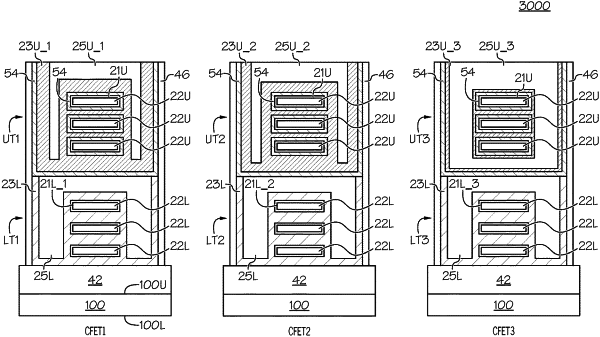
a first complementary field effect transistor (CFET) stack on a substrate, the first CFET stack comprising:
a first upper transistor comprising:
a first upper active region; and
a first upper gate work function layer having a first thickness on the first upper active region; and
a first lower transistor comprising:
a first lower active region;
a first lower gate insulator comprising first dipole elements at a first areal density; and
a first lower gate work function layer on the first lower gate insulator; and
a second CFET stack on the substrate, the second CFET stack comprising:
a second upper transistor comprising:
a second upper active region; and
a second upper gate work function layer having a second thickness on the second upper active region; and
a second lower transistor comprising:
a second lower active region;
a second lower gate insulator comprising second dipole elements at a second areal density; and
a second lower gate work function layer on the second lower gate insulator, wherein the first dipole elements and the second dipole elements have different conductivity types, or the first areal density is different from the second areal density when the first dipole elements and the second dipole elements have the same conductivity type, and
the first thickness is different from the second thickness.
|