| CPC H01L 27/0886 (2013.01) [H01L 21/3086 (2013.01); H01L 21/823431 (2013.01); H01L 21/823437 (2013.01); H01L 21/823468 (2013.01); H01L 21/823481 (2013.01); H01L 29/0673 (2013.01); H01L 29/0847 (2013.01); H01L 29/66545 (2013.01); H01L 29/66795 (2013.01); H01L 29/7851 (2013.01)] | 20 Claims |

|
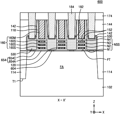
1. An integrated circuit device comprising:
a fin-type active area protruding from a substrate and extending in a first horizontal direction;
a first nanosheet disposed above an upper surface of the fin-type active area with a first separation space therebetween;
a second nanosheet disposed above the first nanosheet with a second separation space therebetween;
a gate line extending on the substrate in a second horizontal direction intersecting the first horizontal direction, the gate line having a sub-gate portion disposed in the second separation space;
a source/drain region disposed on the fin-type active area and in contact with the first nanosheet and the second nanosheet, a first level of a lower surface of the source/drain region being higher than a second level of the upper surface of the fin-type active area; and
a bottom insulation structure disposed in the first separation space,
wherein no portion of the gate line is disposed in the first separation space.
|