| CPC H01L 25/0657 (2013.01) [H01L 23/13 (2013.01); H01L 23/3157 (2013.01); H01L 23/49822 (2013.01); H01L 23/49838 (2013.01); H01L 25/50 (2013.01); H01L 2225/06513 (2013.01); H01L 2225/06541 (2013.01); H01L 2225/06586 (2013.01)] | 20 Claims |

|
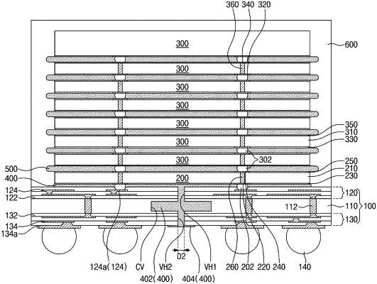
1. A semiconductor package, comprising:
a package substrate;
a cavity in the package substrate;
a first vent hole extending from a top surface of the package substrate to the cavity such that the first vent hole is in fluid communication with the cavity;
a second vent hole extending from a bottom surface of the package substrate to the cavity such that the second vent hole is in fluid communication with the cavity;
a first semiconductor chip mounted on the package substrate;
a second semiconductor chip mounted on the first semiconductor chip; and
a first under-fill layer filling a space between the package substrate and the first semiconductor chip,
wherein the first under-fill layer extending along the first vent hole, the cavity, and the second vent hole onto the bottom surface of the package substrate, and
wherein a width of the cavity is greater than a width of the first vent hole and a width of the second vent hole.
|