| CPC H01L 24/26 (2013.01) [H01L 24/29 (2013.01); H01L 24/32 (2013.01); H01L 24/83 (2013.01); H01L 25/18 (2013.01); H01L 2224/2612 (2013.01); H01L 2224/29082 (2013.01); H01L 2224/2939 (2013.01); H01L 2224/29439 (2013.01); H01L 2224/29455 (2013.01); H01L 2224/2949 (2013.01); H01L 2224/29499 (2013.01); H01L 2224/32145 (2013.01); H01L 2224/83007 (2013.01); H01L 2224/83143 (2013.01); H01L 2224/83203 (2013.01); H01L 2224/83851 (2013.01); H01L 2924/01064 (2013.01); H01L 2924/01065 (2013.01); H01L 2924/01066 (2013.01); H01L 2924/01067 (2013.01); H01L 2924/2075 (2013.01); H01L 2924/20751 (2013.01); H10K 59/131 (2023.02)] | 16 Claims |

|
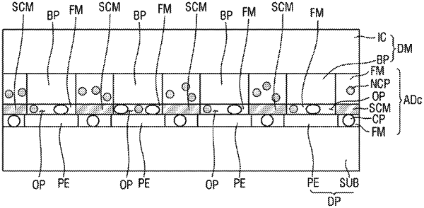
1. An adhesive member comprising:
a conductive particle layer including a plurality of conductive particles;
a non-conductive layer disposed on the conductive particle layer; and
a screening layer interposed between the conductive particle layer and the non-conductive layer and includes a plurality of screening members spaced apart from each other,
wherein the plurality of screening members vertically overlap gaps that are between a plurality of bumps of a driver member configured to drive the pixel circuits of a display panel.
|