| CPC H01L 24/05 (2013.01) [H01L 23/5226 (2013.01); H10B 41/27 (2023.02); H10B 41/41 (2023.02); H10B 43/27 (2023.02); H10B 43/40 (2023.02); H01L 2224/05025 (2013.01)] | 9 Claims |

|
1. A semiconductor memory device comprising:
a substrate;
a memory cell array disposed to be separated from the substrate in a first direction intersecting with a surface of the substrate; and
a plurality of first bonding pad electrodes arranged in a second direction intersecting with the first direction, the plurality of first bonding pad electrodes being disposed at positions away from the memory cell array in a third direction intersecting with the first direction and the second direction, the plurality of first bonding pad electrodes being usable for an input of data to be written to the memory cell array and an output of data read from the memory cell array, wherein
the substrate includes a plurality of first regions and a plurality of second regions arranged alternately in the second direction,
the memory cell array includes:
a plurality of conductive layers that extend in the second direction across the plurality of first regions and the plurality of second regions, the plurality of conductive layers being arranged in the first direction;
a plurality of semiconductor layers disposed in the plurality of first regions, the plurality of semiconductor layers extending in the first direction and being opposed to the plurality of conductive layers; and
a plurality of first contacts disposed in the plurality of second regions, the plurality of first contacts extending in the first direction, the plurality of first contacts having one ends in the first direction closer to the substrate than the plurality of conductive layers and other ends in the first direction farther from the substrate than the plurality of conductive layers, wherein
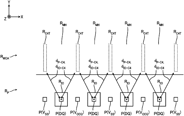
when a distance in the second direction and the third direction between a center position in the second direction and the third direction of a first bonding pad electrode of one of the plurality of first bonding pad electrodes and a center position in the second direction and the third direction of a first contact of the plurality of first contacts closest to the first bonding pad electrode is defined as a first distance,
a difference between a largest first distance and a smallest first distance among a plurality of first distances corresponding to the plurality of first bonding pad electrodes is 400 nm or less.
|