| CPC H01L 23/544 (2013.01) [B23K 26/352 (2015.10); H01L 21/4853 (2013.01); H01L 21/4857 (2013.01); H01L 21/565 (2013.01); H01L 21/568 (2013.01); H01L 23/3128 (2013.01); H01L 23/5383 (2013.01); H01L 23/5386 (2013.01); H01L 23/5389 (2013.01); H01L 23/562 (2013.01); H01L 24/19 (2013.01); H01L 24/20 (2013.01); B23K 2101/40 (2018.08); H01L 2223/54406 (2013.01); H01L 2224/214 (2013.01)] | 20 Claims |

|
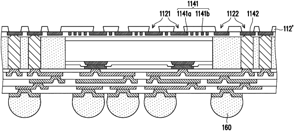
1. A method of manufacturing a semiconductor package, comprising:
forming a backside redistribution structure on a carrier, comprising:
forming a first dielectric layer on the carrier; and
forming a redistribution circuit layer having a circuit pattern and a dummy pattern electrically insulated from the circuit pattern;
forming an encapsulated semiconductor device on the backside redistribution structure, wherein the encapsulated semiconductor device comprises an encapsulating material and a semiconductor device encapsulated by the encapsulating material, and the semiconductor device is overlapped with the dummy pattern from a top view of the semiconductor package;
forming a front side redistribution structure on the encapsulated semiconductor device, wherein the front side redistribution structure is electrically connected to the semiconductor device;
removing the carrier from the first dielectric layer;
performing a patterning process on the first dielectric layer to form a first patterned dielectric layer comprising a marking pattern opening to expose a part of the dummy pattern.
|
|
9. A method of manufacturing a semiconductor package, comprising:
forming a backside redistribution structure, wherein the backside redistribution structure comprises a first dielectric layer, and a redistribution circuit layer over the first dielectric layer, wherein the redistribution circuit layer comprises a plurality of first dummy pads and a plurality of second dummy pads disposed between the first dummy pads, and a size of each of the first dummy pads is substantially greater than a size of each of the second dummy pads;
forming an encapsulated semiconductor device on the backside redistribution structure;
forming a front side redistribution structure on the encapsulated semiconductor device, wherein the front side redistribution structure is electrically connected to the semiconductor device; and
performing a patterning process on the first dielectric layer to form a marking pattern opening partially exposing one of the plurality of first dummy pads.
|
|
16. A method of manufacturing a semiconductor package, comprising:
forming a backside redistribution structure, wherein the backside redistribution structure comprises a first dielectric layer, and a redistribution metal layer over the first dielectric layer and comprising a dummy pattern;
providing a semiconductor device over the backside redistribution structure, wherein an active surface of the semiconductor device faces away from the backside redistribution structure, the semiconductor device is electrically insulated from the dummy pattern and overlapped with the dummy pattern from a top view of the semiconductor package;
forming a front side redistribution structure over the semiconductor device, wherein the front side redistribution structure is electrically connected to the semiconductor device; and
performing a patterning process on the first dielectric layer to form a marking pattern opening exposing a part of the dummy pattern.
|