| CPC H01L 23/544 (2013.01) [G03F 7/70483 (2013.01); H01L 22/32 (2013.01); H01L 23/528 (2013.01)] | 20 Claims |

|
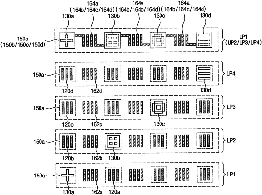
1. A semiconductor device, comprising:
a substrate;
a first lower pattern group on the substrate, wherein the first lower pattern group comprises a first key pattern and a plurality of first lower test patterns that are horizontally spaced apart from the first key pattern; and
a first upper pattern group on the first lower pattern group, wherein the first upper pattern group comprises a plurality of first pads that are horizontally spaced apart from each other and a plurality of first upper test patterns between adjacent ones of the plurality of first pads,
wherein the first key pattern is configured to be used for a photography process associated with fabrication of the semiconductor device,
wherein the plurality of first pads are electrically connected to the plurality of first upper test patterns, and
wherein one of the plurality of first pads vertically overlaps with the first key pattern.
|