| CPC H01L 23/5383 (2013.01) [H01L 21/4857 (2013.01); H01L 23/5386 (2013.01); H01L 25/0652 (2013.01); H01L 25/105 (2013.01); H01L 2225/06513 (2013.01); H01L 2225/06517 (2013.01); H01L 2225/06541 (2013.01); H01L 2225/06586 (2013.01); H01L 2225/06589 (2013.01); H01L 2225/1035 (2013.01); H01L 2225/1041 (2013.01); H01L 2225/1058 (2013.01)] | 20 Claims |

|
1. A semiconductor package, comprising:
a redistribution substrate including a plurality of redistribution line patterns in a dielectric layer; and
a semiconductor chip on the redistribution substrate, the semiconductor chip including a plurality of chip pads electrically connected to the redistribution line patterns,
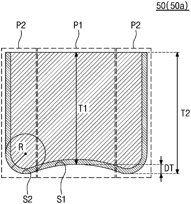
wherein each of the redistribution line patterns includes a substantially planar top surface and a nonplanar bottom surface,
wherein each of the redistribution line patterns includes a central portion and edge portions on opposite sides of the central portion, and each of the redistribution line patterns has a first thickness as a minimum thickness at the central portion and a second thickness as a maximum thickness at the edge portions,
wherein the first thickness and the second thickness are measured in a direction perpendicular to a top surface of the dielectric layer, and
wherein the nonplanar bottom surface is in direct contact with the dielectric layer.
|