| CPC H01L 23/528 (2013.01) [H01L 23/53228 (2013.01); H01L 27/088 (2013.01)] | 11 Claims |

|
1. A semiconductor device comprising:
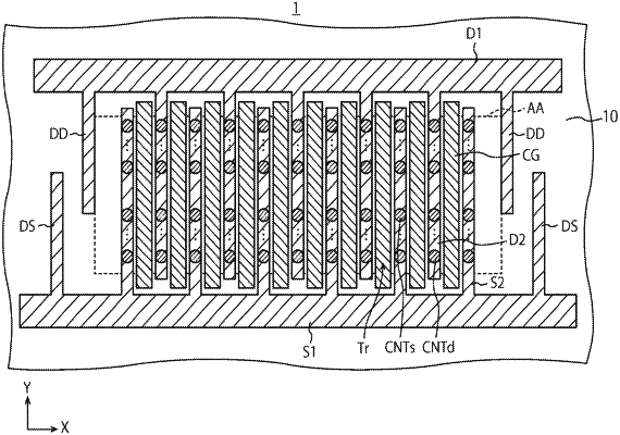
a first source line provided above a substrate and extending in a first direction with a first width in a plan view of the device;
at least one second source line connected to the first source line and extending in a second direction from the first source line with a second width that is smaller than the first width in the plan view;
a dummy source line arranged adjacently to the at least one second source line in the plan view, connected to the first source line, and extending in the second direction from the first source line in the plan view while not electrically connected to lines other than the first source line;
a first drain line provided above the substrate and extending in the first direction with a third width in a plan view of the device;
at least one second drain line connected to the first drain line and extending in the second direction from the first drain line with a fourth width that is smaller than the third width in the plan view;
a dummy drain line arranged adjacently to the at least one second drain line in the plan view, connected to the first drain line, and extending in the second direction from the first drain line in the plan view while not electrically connected to lines other than the first drain line; and
a gate electrode provided between the second source line and the second drain line.
|