| CPC H01L 23/49838 (2013.01) [H01L 23/49827 (2013.01); H05K 1/0296 (2013.01)] | 10 Claims |

|
1. A wiring substrate comprising:
an insulation substrate that comprises a recess section in a first surface, a frame portion that forms a side surface which connects an opened surface of the recess section and a bottom surface of the recess section to each other, and a base portion that forms the bottom surface; and
an electrical wiring structure that is on and inside the base portion,
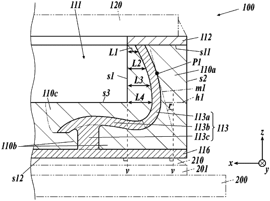
wherein the frame portion comprises a first conductive portion having a plate shape in the frame portion, and extending from the first surface to the base portion through the frame portion,
wherein the first conductive portion is coated with an insulation body, and
wherein a distance between the first conductive portion and an inner side surface of the recess section is greater at a bottom surface height of the recess section than on a first surface side.
|