| CPC H01L 23/49838 (2013.01) [H01L 21/4853 (2013.01); H01L 21/486 (2013.01); H01L 21/6835 (2013.01); H01L 23/49811 (2013.01); H01L 23/49827 (2013.01); H01L 23/49866 (2013.01); H01L 24/16 (2013.01); H01L 24/81 (2013.01); H01L 25/0657 (2013.01); H01L 23/3121 (2013.01); H01L 24/13 (2013.01); H01L 24/17 (2013.01); H01L 25/18 (2013.01); H01L 2221/68345 (2013.01); H01L 2221/68359 (2013.01); H01L 2224/13111 (2013.01); H01L 2224/13139 (2013.01); H01L 2224/13147 (2013.01); H01L 2224/16146 (2013.01); H01L 2224/16238 (2013.01); H01L 2224/16503 (2013.01); H01L 2224/17181 (2013.01); H01L 2224/81005 (2013.01); H01L 2225/06513 (2013.01); H01L 2225/06517 (2013.01); H01L 2225/06541 (2013.01); H01L 2225/06565 (2013.01); H01L 2225/06582 (2013.01); H01L 2924/01028 (2013.01); H01L 2924/01327 (2013.01); H01L 2924/014 (2013.01); H01L 2924/1438 (2013.01); H01L 2924/14511 (2013.01)] | 4 Claims |

|
1. A method for manufacturing a semiconductor device, comprising:
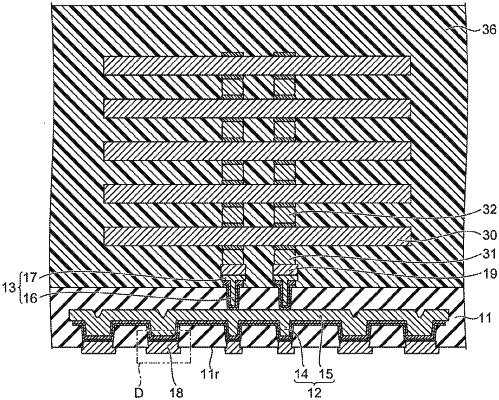
forming a release layer, a first barrier layer, a conductive layer, and a second barrier layer on a support substrate;
forming a first insulating layer on the second barrier layer, a first opening being formed in the first insulating layer;
forming a second opening in the second barrier layer by etching using the first insulating layer as a mask, the second opening communicating with the first opening;
forming a first electrode inside the second opening and inside a lower portion of the first opening;
forming a third barrier layer on an inner surface of an upper portion of the first opening;
forming a first via inside an upper portion of the first opening and forming an interconnect on the first insulating layer, a resistivity of the interconnect being lower than a resistivity of the third barrier layer;
forming a second insulating layer on the interconnect, a third opening being formed in the second insulating layer;
forming a second via inside the third opening, the second via being connected to the interconnect;
forming a second electrode on the second via, the second electrode being connected to the second via;
connecting a chip to the second electrode;
removing the support substrate by removing the release layer; and
removing the first barrier layer, the conductive layer, and the second barrier layer.
|