| CPC H01L 23/49811 (2013.01) [H01L 21/4853 (2013.01); H01L 21/4882 (2013.01); H01L 23/3121 (2013.01); H01L 23/367 (2013.01); H01L 24/05 (2013.01); H01L 24/43 (2013.01); H01L 24/45 (2013.01); H01L 25/16 (2013.01); H01L 2924/1304 (2013.01)] | 18 Claims |

|
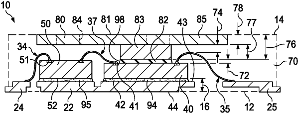
1. A semiconductor package comprising:
a metallic pad, a first set of leads and a second set of leads;
a first semiconductor die and a second semiconductor die attached to the metallic pad, the first semiconductor die electrically connected to the first set of leads and the second semiconductor die electrically connected to the second set of leads, and the first semiconductor die electrically connected to the second semiconductor die, wherein the first semiconductor die is configured to control switching of transistors in the second semiconductor die;
a heat spreader attached to the second semiconductor die via an electrically insulating material, wherein the heat spreader includes an exposed pad and a protrusion extending from the exposed pad;
a mold compound covering portions of the first semiconductor die, the second semiconductor die, the metallic pad, and the heat spreader.
|