| CPC H01L 23/498 (2013.01) [H01L 23/49866 (2013.01); H01L 23/522 (2013.01); H01L 23/53238 (2013.01); H01L 24/05 (2013.01); H01L 24/06 (2013.01); H01L 24/08 (2013.01); H01L 24/09 (2013.01); H01L 25/0657 (2013.01); H01L 25/50 (2013.01); H01L 27/14634 (2013.01); H01L 27/14636 (2013.01); H01L 27/1464 (2013.01); H01L 24/80 (2013.01); H01L 2224/05547 (2013.01); H01L 2224/05571 (2013.01); H01L 2224/0603 (2013.01); H01L 2224/06131 (2013.01); H01L 2224/06133 (2013.01); H01L 2224/0616 (2013.01); H01L 2224/06517 (2013.01); H01L 2224/08123 (2013.01); H01L 2224/08147 (2013.01); H01L 2224/09517 (2013.01); H01L 2224/80194 (2013.01); H01L 2224/80357 (2013.01); H01L 2224/80895 (2013.01); H01L 2224/80896 (2013.01); H01L 2225/06513 (2013.01); H01L 2225/06565 (2013.01); H01L 2924/00012 (2013.01); H01L 2924/00014 (2013.01); H01L 2924/01029 (2013.01); H01L 2924/12043 (2013.01); H01L 2924/13091 (2013.01)] | 9 Claims |

|
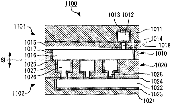
1. A semiconductor device, comprising:
a first section including a first electrode extending in a first direction; and
a second section including a second electrode and disposed to be bonded to the first section at a bonding interface, the second electrode being bonded to the first electrode at the bonding interface and extending in a second direction that intersects with the first direction.
|