| CPC H01L 23/49575 (2013.01) [H01L 23/3107 (2013.01); H01L 23/49506 (2013.01); H01L 23/4952 (2013.01); H01L 23/49562 (2013.01); H01L 23/49568 (2013.01); H01L 23/49589 (2013.01); H01L 23/50 (2013.01)] | 8 Claims |

|
1. A semiconductor module comprising:
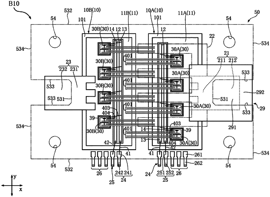
a semiconductor device that includes: an insulating substrate having a main surface and a back surface that face opposite to each other in a thickness direction; a conductive member arranged on the main surface; a plurality of switching elements electrically connected to the conductive member; a first input terminal, having a first terminal portion that includes a first planar surface and a second planar surface opposite to each other, and electrically connected to the conductive member; and a second input terminal having a second terminal portion overlapping with the first terminal portion as viewed in a normal direction of the first planar surface of the first terminal portion, the second input terminal being spaced apart from the first input terminal and the conductive member in the normal direction of the first planar surface of the first terminal portion and electrically connected to the plurality of switching elements; and
a bus bar that includes a first supply terminal that includes a third planar surface and a fourth planar surface opposite to each other; and a second supply terminal spaced apart from the first supply terminal in a normal direction of the third planar surface of the first supply terminal, the second supply terminal at least partially overlapping with the first supply terminal as viewed in the normal direction of the fourth planar surface of the first supply terminal,
wherein the first supply terminal is electrically connected to the first terminal portion, and
the second supply terminal is electrically connected to the second terminal portion.
|