| CPC H01L 23/49575 (2013.01) [H01L 23/3142 (2013.01); H01L 24/48 (2013.01); H01L 24/85 (2013.01); H01L 25/0655 (2013.01); H01L 2224/48137 (2013.01); H01L 2224/48247 (2013.01); H01L 2924/181 (2013.01)] | 20 Claims |

|
1. A semiconductor device comprising:
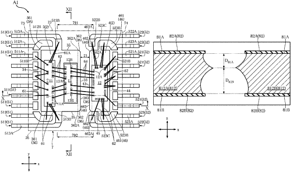
a conductive support member including a first die pad and a second die pad, which are separated from each other in a first direction orthogonal to a thickness direction and have relatively different potentials from each other;
a first semiconductor element that is mounted on the first die pad and forms a first circuit together with the first die pad;
a second semiconductor element that is mounted on the second die pad and forms a second circuit together with the second die pad;
an insulating element that conducts to the first semiconductor element and the second semiconductor element and insulates the first circuit and the second circuit from each other; and
a sealing resin that covers the first die pad, the second die pad, the first semiconductor element, the second semiconductor element, and the insulating element and insulates the first die pad and the second die pad from each other,
wherein the first die pad and the second die pad overlap each other when viewed along the first direction,
wherein the first die pad has a first main surface, which faces the thickness direction and on which the first semiconductor element is mounted, and a first back surface facing an opposite side to the first main surface in the thickness direction,
wherein the second die pad has a second main surface, which faces the thickness direction and on which the second semiconductor element is mounted, and a second back surface facing an opposite side to the second main surface in the thickness direction, and
wherein when viewed along a second direction orthogonal to both the thickness direction and the first direction, a distance in the first direction between the first back surface and the second back surface is larger than a distance in the first direction between the first main surface and the second main surface.
|