US 11,923,256 B2
Cap for package of integrated circuit
Olivier Franiatte, Grenoble (FR); and Richard Rembert, Quaix en Chartreuse (FR)
Assigned to STMicroelectronics (Grenoble 2) SAS, Grenoble (FR)
Filed by STMicroelectronics (Grenoble 2) SAS, Grenoble (FR)
Filed on Jul. 16, 2021, as Appl. No. 17/378,398.
Application 17/378,398 is a division of application No. 16/551,241, filed on Aug. 26, 2019, granted, now 11,101,188.
Claims priority of application No. 1857919 (FR), filed on Sep. 4, 2018.
Prior Publication US 2021/0343609 A1, Nov. 4, 2021
Int. Cl. H01L 23/538 (2006.01); H01L 21/56 (2006.01); H01L 23/04 (2006.01); H01L 23/498 (2006.01); H01L 21/60 (2006.01); H01L 21/603 (2006.01)
CPC H01L 23/04 (2013.01) [H01L 21/56 (2013.01); H01L 23/49816 (2013.01); H01L 23/5385 (2013.01); H01L 2021/60022 (2013.01); H01L 21/603 (2021.08)] 22 Claims
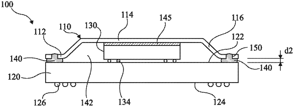
OG exemplary drawing
 
1. A method of packaging a semiconductor chip, the method comprising:
soldering the chip to a substrate;
arranging a cover over the substrate and the chip, the cover including a central plate overlying the chip and a peripheral frame surrounding the central plate, the peripheral frame including through openings formed therein; and
gluing the peripheral frame to peripheral regions of the substrate so that glue is formed in the through openings.