| CPC H01L 21/76283 (2013.01) [H01L 21/02002 (2013.01); H01L 21/76224 (2013.01); H01L 21/84 (2013.01); H01L 27/1203 (2013.01); H01L 27/1218 (2013.01); H01L 29/0649 (2013.01); H01L 29/78603 (2013.01); H01L 21/76264 (2013.01)] | 20 Claims |

|
1. A substrate for microelectronic radiofrequency devices comprising:
a support substrate comprising a first semiconductor material having a resistivity greater than 500 ohms·cm;
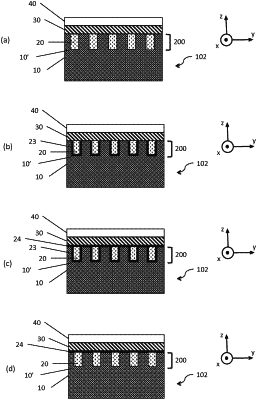
a plurality of trenches in a region of the support substrate filled with a second material and defining a plurality of first zones on a first side of the first semiconductor material and at least one second zone of a second material, the second material having a resistivity greater than 10 kohms·cm, the plurality of first zones having a maximum lateral dimension of less than 10 microns, the plurality of first zones being isolated from one another by the at least one second zone;
a useful layer comprising a material selected from a group consisting of a semiconductor material, a conductive material, or a piezoelectric material located above an upper surface of the support substrate along a lateral extent of the region of the support substrate, the material of the useful layer comprising a continuous portion in two lateral directions and located above each trench of the plurality of trenches; and
an insulating layer located directly between the support substrate and the useful layer in locations above the plurality of trenches, the insulating layer directly on the first semiconductor material and the second material along the lateral extent of the region of the support substrate.
|