| CPC H01F 27/40 (2013.01) [H01F 27/2804 (2013.01); H01F 27/29 (2013.01); H01G 4/005 (2013.01); H01G 4/30 (2013.01); H01F 2027/2809 (2013.01)] | 17 Claims |

|
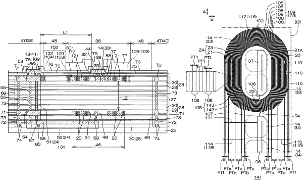
1. An insulation type component comprising:
an insulating layer laminated structure;
a first spiral conductor pattern that is arranged in the insulating layer laminated structure to form a lower coil in a laminated direction;
a second spiral conductor pattern that is arranged in the insulating layer laminated structure to form an upper coil in the laminated direction;
a first inner coil end wiring that is arranged in the insulating layer laminated structure so as to be located in a region surrounded by the first spiral conductor pattern, in plan view, and that is electrically connected to the first spiral conductor pattern; and
a second inner coil end wiring that is arranged in the insulating layer laminated structure so as to be located in a region surrounded by the second spiral conductor pattern, in plan view, and that is electrically connected to the second spiral conductor pattern,
wherein the second spiral conductor pattern includes:
a first upper side spiral pattern that is routed so as to be wound in a first spiral shape, in plan view, surrounding the second inner coil end wiring so as to face the first spiral conductor pattern in the laminated direction of the insulating layer laminated structure and so as not to face the first inner coil end wiring in the laminated direction; and
a second upper side spiral pattern that is continuously routed from the first upper side spiral pattern so as to be wound in a second spiral shape outwardly from the first spiral conductor pattern, in plan view, so as to be electrically and mechanically connected to the first upper side spiral pattern and so as not to face the first spiral conductor pattern in the laminated direction.
|