| CPC H01B 1/12 (2013.01) [C25D 1/04 (2013.01); C25D 5/022 (2013.01); C25D 5/56 (2013.01); H01B 1/22 (2013.01); H05K 1/0393 (2013.01); H05K 3/027 (2013.01); H05K 2201/0108 (2013.01); H05K 2203/107 (2013.01)] | 20 Claims |

|
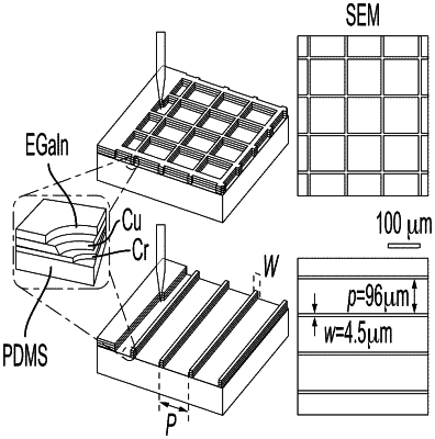
1. A method of manufacturing a stretchable and transparent electronic structure comprising a plurality of laser patterned biphasic metallic grid lines having a thickness up to 600 nanometers and a width up to 6 micrometers, the structure comprising a stretchable elastomer layer, a metal alloying layer on top of the stretchable elastomer layer, and a liquid metal, wherein the structure is colorless and transparent when viewed under visible light, the method comprising:
depositing a metal adhesion layer on the stretchable elastomer layer;
depositing the metal alloying layer on the metal adhesion layer; and
alloying the metal alloying layer and the liquid metal to form an electrically conductive material layer; and
laser patterning a pattern of the electrically conductive material layer to form the biphasic metallic grid lines.
|