| CPC G11C 7/222 (2013.01) [G11C 7/1069 (2013.01); G11C 7/1096 (2013.01); G11C 29/12015 (2013.01); G11C 29/46 (2013.01)] | 20 Claims |

|
1. A memory device comprising:
a first signal pin configured to receive a data clock;
a second signal pin configured to transmit a read clock; and
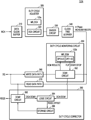
a data clock circuit receiving the data clock and configured to
perform first duty cycle monitoring that monitors a duty cycle of the data clock, generates a first result, and provides a timing-adjusted data clock in response to the first duty cycle monitoring,
perform second duty cycle monitoring that monitors a duty cycle of the read clock, generates a second result, and provides a timing-adjusted read clock in response to the second duty cycle monitoring,
calculate an offset of the read clock in response to the timing-adjusted data clock, the first result and the second result, and
correct a duty error of the read clock using a read clock offset code derived in relation to the offset of the read clock,
wherein the data clock controls data write timing during a write operation executed by the memory device,
the data clock controls data read timing during a read operation executed by the memory device, and
the read clock controls communication of read data from the memory device.
|