| CPC G11C 7/06 (2013.01) [G11C 7/1012 (2013.01); G11C 7/1048 (2013.01); G11C 7/1063 (2013.01); G11C 7/1069 (2013.01); G11C 7/1096 (2013.01); G11C 7/12 (2013.01)] | 18 Claims |

|
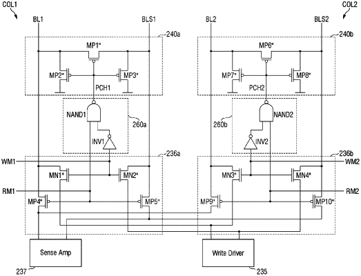
1. A pseudo dual port memory device comprising:
a memory cell;
a pair of bit lines connected to the memory cell;
a write driver;
a sense amp;
a column multiplexer which is connected to the bit lines and configured to receive a write multiplexer control signal and a read multiplexer control signal, the column multiplexer configured to connect the bit lines to the write driver in response to the write multiplexer control signal and configured to connect the bit lines to the sense amp in response to the read multiplexer control signal;
a precharge control signal generation circuit which is connected to the column multiplexer and configured to generate a precharge control signal on the basis of the write multiplexer control signal and the read multiplexer control signal; and
a bit line precharge circuit which is connected to the precharge control signal generation circuit and the pair of bit lines and configured to precharge the bit lines on the basis of the precharge control signal.
|