| CPC G11C 29/44 (2013.01) [G11C 16/10 (2013.01); G11C 16/26 (2013.01); G11C 29/42 (2013.01); G11C 29/50004 (2013.01); G11C 29/783 (2013.01)] | 20 Claims |

|
1. A system comprising:
a memory device;
a processing device operatively coupled with the memory device; and
a memory operatively coupled with the processing device and storing instructions that, when executed by the processing device, cause the processing device to perform operations comprising:
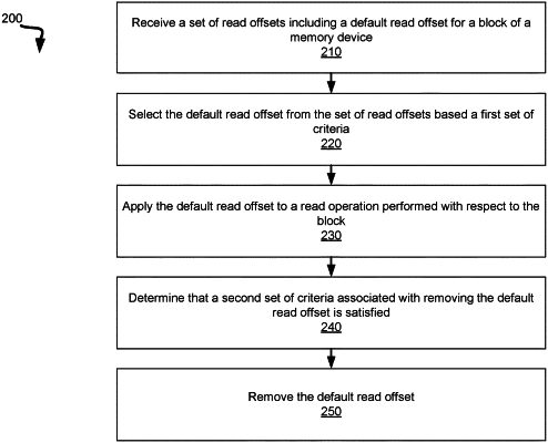
initiating a read operation with respect to a block of the memory device;
selecting, based on a set of criteria, a default read offset from a set of read offsets, wherein the set of criteria comprises at least one of: a parameter related to trigger rate, or an amount of time that an open block is allowed to remain open to control threshold voltage shift due to storage charge loss; and
applying the default read offset to perform the read operation.
|