| CPC G11C 29/42 (2013.01) [G11C 29/1201 (2013.01); G11C 29/18 (2013.01); G11C 29/4401 (2013.01); G11C 29/50004 (2013.01); G11C 2029/1202 (2013.01)] | 12 Claims |

|
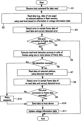
1. A memory system comprising:
a non-volatile memory device; and
a controller configured to execute an error correction process on first data read from a first area at a first address of the non-volatile memory device and determine a read level used for reading data at the first address according to a result of the correction process, wherein
the controller is configured to
execute the correction process on first frame data of the first data using an error correction circuit, and
when the correction process on the first frame data has failed, determine the read level based on estimated data in the error correction circuit.
|