| CPC G11C 16/3459 (2013.01) [G11C 7/04 (2013.01); G11C 16/10 (2013.01); G11C 16/26 (2013.01); G11C 16/32 (2013.01); G11C 16/3404 (2013.01)] | 17 Claims |

|
1. A method comprising:
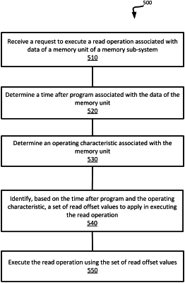
receiving, by a processing device, a request to execute a read operation associated with data of a memory unit of a memory sub-system;
determining a time after program associated with the data;
determining a temperature level associated with the memory unit;
identifying, based on the time after program and the temperature level, a first threshold voltage offset bin of a plurality of threshold voltage offset bins, wherein the first threshold voltage offset bin comprises a set of read offset values to apply in executing the read operation; and
executing the read operation using the set of read offset values.
|