| CPC G11C 16/10 (2013.01) [G06F 3/0614 (2013.01); G06F 3/0631 (2013.01); G06F 3/0652 (2013.01); G06F 3/0659 (2013.01); G06F 3/0665 (2013.01); G06F 3/0679 (2013.01); G06F 12/0246 (2013.01); G11C 11/5635 (2013.01); G11C 16/0483 (2013.01); G11C 16/16 (2013.01); G11C 16/3418 (2013.01); G06F 2212/1032 (2013.01); G06F 2212/152 (2013.01); G06F 2212/214 (2013.01); G06F 2212/7202 (2013.01); G11C 2213/71 (2013.01)] | 12 Claims |

|
1. A storage device comprising:
a bit line;
a source line;
a first memory string including a first select transistor connected to the bit line, a second select transistor connected to the source line, and a plurality of memory cell transistors series-connected between the first select transistor and the second select transistor, the memory cell transistors of the first memory string including
a first memory cell transistor,
a second memory cell transistor between the first memory cell transistor and the first select transistor,
a third memory cell transistor between the second memory cell transistor and the first select transistor,
a fourth memory cell transistor between the third memory cell transistor and the first select transistor, and
a fifth memory cell transistor between the fourth memory cell transistor and the first select transistor;
a second memory string including a third select transistor connected to the bit line, a fourth select transistor connected to the source line, and a plurality of memory cell transistors series-connected between the third select transistor and the fourth select transistor, the memory cell transistors of the second memory string including
a sixth memory cell transistor,
a seventh memory cell transistor between the sixth memory cell transistor and the third select transistor,
an eighth memory cell transistor between the seventh memory cell transistor and the third select transistor,
a ninth memory cell transistor between the eighth memory cell transistor and the third select transistor, and
a tenth memory cell transistor between the ninth memory cell transistor and the third select transistor;
a first select line connected to a gate of the first select transistor;
a second select line connected to a gate of the third select transistor;
a first word line connected to a gate of the first memory cell transistor and a gate of the sixth memory cell transistor;
a second word line connected to a gate of the second memory cell transistor and a gate of the seventh memory cell transistor;
a third word line connected to a gate of the third memory cell transistor and a gate of the eighth memory cell transistor;
a fourth word line connected to a gate of the fourth memory cell transistor and a gate of the ninth memory cell transistor;
a fifth word line connected to a gate of the fifth memory cell transistor and a gate of the tenth memory cell transistor; and
a control circuit configured to
perform an erase operation to erase data stored in the first to tenth memory cell transistors,
perform a first write operation to write first data into the third memory cell transistor after the erase operation, and
perform a second write operation to write second data into the eighth memory cell transistor after the first write operation,
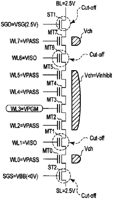
the first write operation including,
supplying a select voltage to the first select line,
supplying non-select voltage to the second select line,
supplying a first program voltage to the third word line,
supplying a first channel-control voltage to the second word line, and
supplying a first pass voltage to the first word line, and the fourth word line,
the non-select voltage being lower than the select voltage, the first channel-control voltage being lower than the first pass voltage, the first pass voltage being lower than the first program voltage and greater than the select voltage, and
the second write operation including,
supplying the non-select voltage to the first select line,
supplying the select voltage to the second select line,
supplying the first program voltage to the third word line,
supplying the first channel-control voltage to the second word line, and
supplying the first pass voltage to the first word line, and the fourth word line.
|