| CPC G11C 11/404 (2013.01) [G11C 11/4096 (2013.01)] | 22 Claims |

|
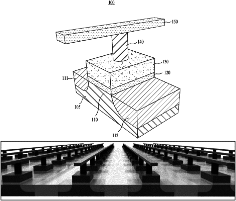
1. A DRAM device comprising:
a channel region formed on a substrate;
a gate insulating film region formed on the channel region;
a floating gate region formed on the gate insulating film region, the floating gate region having a lower surface in contact with the gate insulating film region and an opposing upper surface;
a transition layer region formed on the upper surface of the floating gate region wherein an area of the transition layer that is in contact with the floating gate region is smaller than a total area of the upper surface of the floating gate region; and
a control gate region formed on the transition layer region, wherein the control gate region is configured to:
generate a potential difference with the floating gate region in response to a fact that a potential that is not less than a reference potential is applied; and
release at least one charge stored in the floating gate region or store the at least one charge into the floating gate region, by generating a transition current due to the potential difference.
|