| CPC G09G 3/32 (2013.01) [G06F 3/0412 (2013.01); G06F 3/044 (2013.01); G06F 3/046 (2013.01); G09G 2300/0814 (2013.01); G09G 2310/0202 (2013.01); G09G 2310/0243 (2013.01); G09G 2320/064 (2013.01); G09G 2320/0646 (2013.01); G09G 2354/00 (2013.01)] | 9 Claims |

|
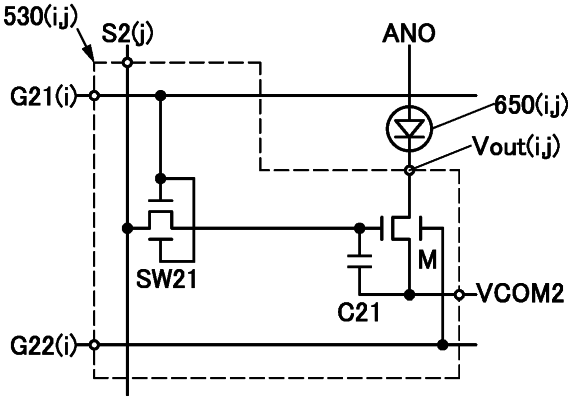
1. A display panel comprising a pixel,
wherein the pixel comprises a pixel circuit and a display element,
wherein the display element is electrically connected to the pixel circuit,
wherein the pixel circuit is supplied with a selection signal, an image signal, and a pulse width control signal,
wherein the pixel circuit is configured to supply an output potential,
wherein the pixel circuit is configured to determine a period during which the output potential is supplied, on the basis of the pulse width control signal,
wherein the pixel circuit comprises a first switch and a first transistor,
wherein the first switch is configured to supply the image signal on the basis of the selection signal,
wherein the first transistor is configured to determine the output potential on the basis of the image signal,
wherein the first switch comprises a first semiconductor film comprising silicon,
wherein the first transistor comprises a first electrode, a second electrode, a first gate electrode, a second gate electrode, and a second semiconductor film, the second semiconductor film comprising an oxide semiconductor,
wherein the output potential is output from the first electrode,
wherein the first gate electrode is supplied with the image signal, and
wherein the second gate electrode is supplied with the pulse width control signal.
|