| CPC G09G 3/006 (2013.01) [H01L 27/124 (2013.01); G09G 2300/0426 (2013.01); G09G 2330/12 (2013.01)] | 19 Claims |

|
1. A display device comprising:
a substrate including a display area and a peripheral area;
a plurality of light-emitting elements positioned in the display area;
a plurality of pixel circuits connected to the plurality of light-emitting elements, respectively;
a sensor positioned on the peripheral area of the substrate;
a leakage current detecting circuit connected to the sensor; and
a light emitting wiring connected to the leakage current detecting circuit and connected to at least one of the plurality of light-emitting elements,
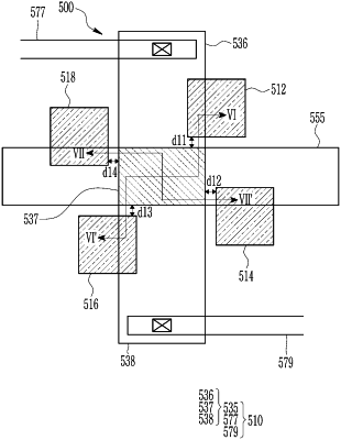
wherein the sensor includes a first sensor, the first sensor includes:
a first sensing transistor, and
a first conductive pattern spaced apart from a channel of the first sensing transistor, the first conductive pattern being a floating pattern, and
wherein the first conductive pattern is positioned in the same layer as at least one of a plurality of layers configuring the plurality of pixel circuits.
|