| CPC G06N 10/00 (2019.01) [H01L 27/088 (2013.01); H01L 29/122 (2013.01); H01L 29/775 (2013.01)] | 20 Claims |

|
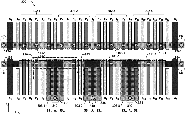
1. A quantum dot device, comprising:
a quantum well stack structure comprising a quantum well stack that includes a quantum dot formation region;
a plurality of gates extending to the quantum dot formation region, wherein the plurality of gates includes a first gate coupled to a first doped region, a second gate coupled to a second doped region, and a third gate coupled to a third doped region, the third gate being between the first gate and the second gate; and
an insulating material over the quantum well stack, the insulating material comprising a first trench extending toward the quantum well stack and a second trench extending toward the quantum well stack, wherein the second trench intersects the first trench, and wherein a gate metal of the third gate has a first portion that is at least partially in the first trench and has a second portion that is at least partially in the second trench.
|