| CPC G06F 3/0659 (2013.01) [G06F 3/0626 (2013.01); G06F 3/0658 (2013.01); G06F 3/0673 (2013.01); G11C 7/1006 (2013.01)] | 20 Claims |

|
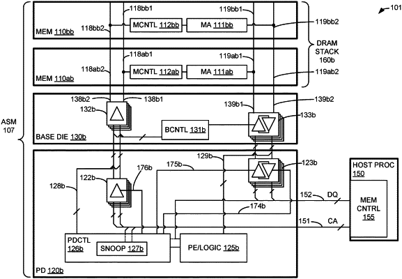
1. An integrated circuit stack, comprising:
an external command/address (CA) interface to receive commands and addresses from a device external to the integrated circuit stack;
a set of stacked memory devices comprising memory cell circuitry, the set of stacked memory devices to receive, via a memory device CA interface, commands and addresses received by the integrated circuit stack via the external CA interface; and,
a processing device electrically coupled to, and stacked with, the set of stacked memory device to form a first device stack, the first processing device comprising at least one processing element, the first processing device to receive, via a processing device CA interface, the commands and addresses received by the integrated circuit stack via the external CA interface, the first processing device to, in response to a first mode setting command received via the processing device CA interface, determine whether the first mode setting command is directed to the processing device.
|