| CPC G06F 3/0619 (2013.01) [G06F 3/0649 (2013.01); G06F 3/0688 (2013.01); G06F 11/1044 (2013.01); G06F 12/0292 (2013.01)] | 13 Claims |

|
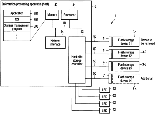
1. A controller connectable to a plurality of storage devices each including a nonvolatile memory, the controller configured to:
send a command to one storage device of the plurality of storage devices, the command being for writing each of data portions corresponding to logical addresses included in a first logical address space to the one storage device of the plurality of storage devices, in accordance with write requests received from a processor;
manage mapping between the logical addresses and addresses indicative of storage locations in the storage devices to which the data portions are written, by using an address translation table; and
when it is determined that a first storage device of the plurality of storage devices is to be removed and an additional storage device including a nonvolatile memory is connected to the controller:
control the first storage device in a first mode in which data write is inhibited and data read is permitted;
execute, in response to receiving, from the processor, first subsequent write requests specifying first logical addresses corresponding to data portions written to the first storage device, first processing of writing first update data portions corresponding to the data portions written to the first storage device, to a storage device selected from the additional storage device and remaining one or more storage devices of the plurality of storage devices except for the first storage device, without writing the first update data portions to the first storage device, and change addresses indicative of storage locations mapped to the first logical addresses in the address translation table from addresses indicative of storage locations in the first storage device to addresses indicative of storage locations in the selected storage device to which the first update data portions are written; and
execute, in response to receiving, from the processor, second subsequent write requests specifying second logical addresses corresponding to data portions written to the remaining one or more storage devices of the plurality of storage devices, second processing of writing second update data portions corresponding to the data portions written to the remaining one or more storage devices, to the selected storage device, and change addresses indicative of storage locations mapped to the second logical addresses in the address translation table from addresses indicative of storage locations in the remaining one or more storage devices to addresses indicative of storage locations in the selected storage device to which the second update data portions are written.
|