US 11,921,944 B2
Touch display panel and touch display device
HoonBae Kim, Seoul (KR); CheolSe Kim, Daegu (KR); SeungMok Shin, Daegu (KR); JuHan Kim, Gyeonggi-do (KR); YongChan Park, Seoul (KR); and HyunHo Park, Gyeongsangbuk-do (KR)
Assigned to LG Display Co., Ltd., Seoul (KR)
Filed by LG Display Co., Ltd., Seoul (KR)
Filed on Sep. 12, 2022, as Appl. No. 17/942,805.
Application 17/942,805 is a continuation of application No. 17/245,652, filed on Apr. 30, 2021, granted, now 11,467,685.
Application 17/245,652 is a continuation of application No. 16/124,998, filed on Sep. 7, 2018, granted, now 11,023,059, issued on Jun. 1, 2021.
Claims priority of application No. 10-2017-0115303 (KR), filed on Sep. 8, 2017; and application No. 10-2018-0081639 (KR), filed on Jul. 13, 2018.
Prior Publication US 2023/0004251 A1, Jan. 5, 2023
This patent is subject to a terminal disclaimer.
Int. Cl. G06F 3/041 (2006.01); G02F 1/1333 (2006.01); G02F 1/136 (2006.01); G06F 3/044 (2006.01); G06F 3/047 (2006.01); G09G 3/20 (2006.01)
CPC G06F 3/0412 (2013.01) [G06F 3/04164 (2019.05); G06F 3/0443 (2019.05); G06F 3/047 (2013.01); G09G 3/2096 (2013.01); G02F 1/13338 (2013.01); G02F 1/13606 (2021.01); G02F 2201/123 (2013.01); G06F 2203/04107 (2013.01); G09G 2354/00 (2013.01)] 14 Claims
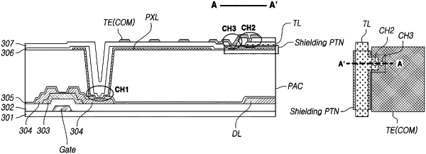
OG exemplary drawing
 
1. A touch display device, comprising:
a touch display panel;
a touch electrode embedded in the touch display panel;
a touch line electrically connected to the touch electrode;
a data line disposed on a layer different from a layer where the touch line is disposed;
a pixel electrode coupled to the data line; and
a shielding structure interposed between the touch line and the data line, and the shielding structure overlapping partially the data line, and the touch electrode in a plan view.