| CPC G06F 13/1668 (2013.01) [G11C 11/4093 (2013.01); G11C 11/4096 (2013.01)] | 20 Claims |

|
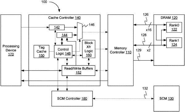
1. A cache controller circuit in a block transfer mode, the cache controller circuit comprising:
a data buffer; and
logic coupled to the data buffer, wherein the logic is to:
transfer first data to a dynamic random access memory (DRAM) device over a first data channel via a memory controller circuit;
send a block read command packet to the DRAM device via the memory controller circuit;
provide a status signal to the memory controller circuit, the status signal to indicate that a second data channel between the memory controller circuit and the DRAM device is activated to perform a data transfer with a first rank of the DRAM device on behalf of a second memory device while the first data is being transferred across the first data channel between the memory controller circuit and the DRAM device;
cause the DRAM device to enable an auxiliary data port and block read logic of the DRAM device; and
receive second data over the second data channel from the auxiliary data port; and
store the second data in the data buffer.
|