| CPC G06F 11/1068 (2013.01) [G06F 3/0619 (2013.01); G06F 3/0659 (2013.01); G06F 3/0679 (2013.01); G06F 11/076 (2013.01); G06F 11/0772 (2013.01)] | 17 Claims |

|
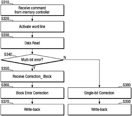
1. A method of operating a memory device, the method comprising:
receiving a first command from a controller;
activating a page of a memory cell array based on the first command;
reading data of the activated page;
detecting an error from the read data;
correcting the detected error to generate error correction data;
writing back the error correction data to the activated page based on the detected error being a single-bit error; and
controlling an error correction circuit of the memory device to receive a second command of blocking the write-back from the controller based on the detected error being a multi-bit error and to block write-back of the error correction data to the activated page based on the second command.
|