| CPC G03F 1/36 (2013.01) [H01L 21/823487 (2013.01)] | 18 Claims |

|
1. A method of fabricating a semiconductor device, the method comprising:
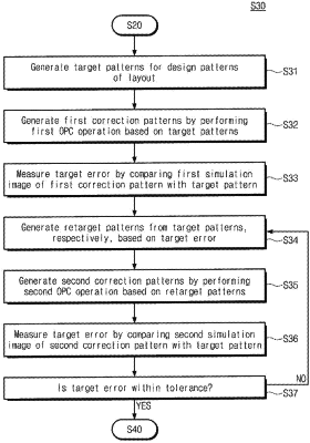
performing an optical proximity correction (OPC) operation on a design pattern of a layout; and
forming a photoresist pattern on a substrate, using a photomask which is manufactured with the layout corrected by the OPC operation,
wherein the OPC operation comprises:
generating a target pattern based on the design pattern;
performing a first OPC operation, based on the target pattern, to generate a first correction pattern;
measuring a first target error by comparing a first simulation image of the first correction pattern with the target pattern;
generating a retarget pattern from the target pattern, based on the first target error; and
performing a second OPC operation, based on the retarget pattern, to generate a second correction pattern,
wherein the method further comprises:
alternately stacking insulating layers and sacrificial layers on the substrate to form a stack;
forming channel holes to penetrate the stack;
forming a respective vertical channel structure in each of the channel holes; and
replacing each of the sacrificial layers with a respective electrode, and
wherein the photoresist pattern defines a mask to form the channel holes.
|