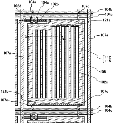
| CPC G02F 1/134309 (2013.01) [G02F 1/133345 (2013.01); G02F 1/133514 (2013.01); G02F 1/1337 (2013.01); G02F 1/134363 (2013.01); G02F 1/13439 (2013.01); G02F 1/136213 (2013.01); G02F 1/136286 (2013.01); G02F 1/1368 (2013.01); H01L 27/1225 (2013.01); H01L 27/124 (2013.01); H01L 27/1255 (2013.01); H01L 29/7869 (2013.01); H01L 29/78696 (2013.01); G02F 1/1362 (2013.01); H01L 2924/0002 (2013.01)] | 2 Claims |

|
2. A semiconductor device comprising:
a first transistor;
a second transistor;
a capacitor;
a first pixel electrode; and
a second pixel electrode,
wherein one of a source and a drain of the first transistor is electrically connected to the first pixel electrode and the capacitor,
wherein one of a source and a drain of the second transistor is electrically connected to the second pixel electrode,
wherein the other of the source and the drain of the first transistor is electrically connected to a source line,
wherein the other of the source and the drain of the second transistor is electrically connected to the source line,
wherein a gate line comprises a region serving as a gate of the second transistor,
wherein a wiring comprises a first region and a second region,
wherein the gate line and the first region extend along the same direction,
wherein the second region has a width larger than a width of the first region,
wherein the second region is configured to be one electrode of the capacitor,
wherein a first conductive layer and the wiring overlap with each other,
wherein the first conductive layer and the gate line overlap with each other,
wherein the first conductive layer and a second conductive layer overlap with each other,
wherein the wiring is electrically connected to the second conductive layer through the first conductive layer,
wherein the second conductive layer and the second pixel electrode overlap with each other,
wherein the first conductive layer comprises the same material with the source line,
wherein the first conductive layer and the first pixel electrode do not overlap with each other, and
wherein the first conductive layer and the second pixel electrode do not overlap with each other.
|