| CPC G01R 31/3177 (2013.01) [G01R 1/07314 (2013.01); G01R 23/165 (2013.01); G01R 25/04 (2013.01); G01R 31/31713 (2013.01); G01R 31/31715 (2013.01); G01R 31/31724 (2013.01); G01R 31/31725 (2013.01); G01R 31/318328 (2013.01); G04F 10/005 (2013.01)] | 20 Claims |

|
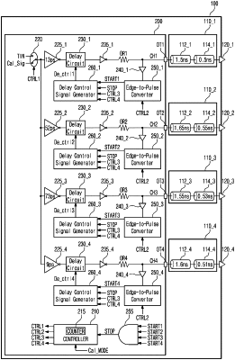
1. A fan-out buffer comprising:
a first channel including a first delay circuit configured to adjust a first delay time of a calibration test signal depending on a first delay control signal;
a second channel including a second delay circuit configured to adjust a second delay time of the calibration test signal depending on a second delay control signal;
a first edge-to-pulse converter configured to detect a first edge included in a first time domain reflectometry (TDR) waveform of an output terminal of the first channel and to generate a first start pulse signal including a first pulse;
a second edge-to-pulse converter configured to detect a first edge included in a second TDR waveform of an output terminal of the second channel and to generate a second start pulse signal including a second pulse;
a stop pulse signal generator configured to generate a stop pulse signal including a first stop pulse by performing an AND operation on the first pulse and the second pulse; and
a first delay control signal generator configured to calculate a phase difference between the first pulse and the first stop pulse and to generate the first delay control signal by using a calculation result such that a skew between the first pulse and the second pulse is calibrated.
|