| CPC G01J 3/2823 (2013.01) [G01J 3/0208 (2013.01); G01J 3/0229 (2013.01); G01J 3/18 (2013.01); G01J 3/4412 (2013.01)] | 21 Claims |

|
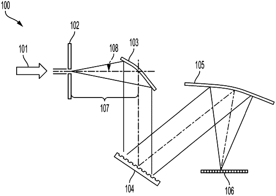
1. An image sensor, comprising:
an aperture;
a dispersion array;
a lens;
an image sensor; and
a processor,
wherein, the dispersion array further comprises a first dispersion structure including a scattering layer and a dispersion layer, wherein the scattering layer includes a first row of nanostructures for scattering light of a first wavelength range, and the dispersion layer is configured to disperse light of a second wavelength range,
wherein the first row of nanostructures is positioned at a first angle different from a second angle of a second row of nanostructures associated with a second dispersion structure of the dispersion array.
|