| CPC H03K 19/0013 (2013.01) [H03K 19/0016 (2013.01)] | 10 Claims |

|
[ 24. An integrated circuit comprising:
two power supply terminals configured to power the integrated circuit, said power supply terminals including a Vdd positive supply terminal and a Vss ground terminal together defining a range of logic levels;
a logic component, the logic component being either a logic gate or a storage cell;
a sleep transistor in series with the logic component and an electrical connection to one of said power supply terminals;
a voltage generator configured to selectively generate a voltage outside said range of logic levels for application to said sleep transistor during a power down mode, and another voltage outside the range of logic levels for application to said sleep transistor when in a mode other than said power down mode, responsive to an enable signal; and
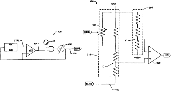
a control circuit configured to control said voltage generator to adequately minimize leakage current through said sleep transistor during said power down mode, comprising:
a first voltage divider configured to provide a voltage reference;
a second voltage divider configured to provide a variable voltage reference responsive to said voltage outside said range of logic levels; and
a comparator having a first input coupled to receive the voltage reference from the first voltage divider, a second input coupled to receive the variable voltage reference from the second voltage divider, and an output coupled to provide the enable signal to the voltage generator. ]
|