| CPC H10K 59/131 (2023.02) [H10K 50/865 (2023.02); H10K 71/00 (2023.02)] | 8 Claims |
|
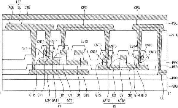
1. A method of manufacturing a display device, comprising:
forming a light blocking pattern on a substrate;
forming an active pattern on the light blocking pattern;
forming a preliminary gate insulating layer covering the active pattern on the substrate;
forming a preliminary gate metal layer on the preliminary gate insulating layer;
patterning the preliminary gate metal layer to concurrently form a gate electrode and an etch stopper;
patterning the preliminary gate insulating layer to concurrently form a first insulating pattern and a second insulating pattern;
forming an insulating layer covering the gate electrode and the etch stopper on the substrate;
forming a first contact hole penetrating the insulating layer, and exposing the etch stopper;
forming a second contact hole penetrating the etch stopper, and being connected to the first contact hole;
forming a third contact hole and a fourth contact hole concurrently, the third contact hole exposing the active pattern and being connected to the second contact hole, and the fourth contact hole exposing the gate electrode; and
forming a first electrode on the insulating layer, the first electrode contacting the active pattern through the first contact hole, the second contact hole, and the third contact hole.
|