| CPC H10K 59/122 (2023.02) [H10K 59/123 (2023.02); H10K 71/00 (2023.02); H10K 2102/103 (2023.02)] | 20 Claims |
|
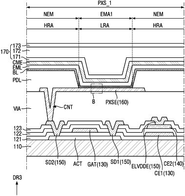
1. A display device comprising:
a light-emitting element comprising:
a pixel electrode including silver,
a common electrode facing the pixel electrode, and
an emission layer between the pixel electrode and the common electrode,
a pixel-defining layer which is between the pixel electrode and the emission layer and exposes the pixel electrode to outside the pixel-defining layer; and
a barrier layer which is between the pixel-defining layer and the emission layer, the barrier layer comprising:
a low-resistance area corresponding to the pixel electrode and having an electrical resistance, and
a high-resistance area extended from the low-resistance area, corresponding to the pixel-defining layer and having an electrical resistance which is higher than the electrical resistance of the low-resistance area.
|