| CPC H10B 43/50 (2023.02) [H01L 21/76877 (2013.01); H01L 23/5226 (2013.01); H10B 41/27 (2023.02); H10B 41/35 (2023.02); H10B 41/50 (2023.02); H10B 43/27 (2023.02); H10B 43/35 (2023.02)] | 19 Claims |

|
1. A semiconductor device comprising:
a three-dimensional (3D) array of memory cells; and
a plurality of common source lines (CSLs) configured to separate the 3D array of memory cells into a plurality of portions, each portion of the plurality of portions being between two adjacent CSLs and comprising:
a plurality of conductive layers separated from each other by insulating layers; and
a plurality of vertical channels arranged orthogonally through the plurality of conductive layers and the insulating layers, each of the plurality of vertical channels comprising a string of memory cells,
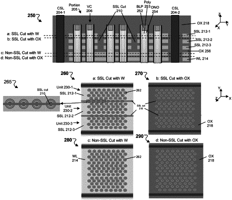
wherein a top part of each portion of one or more portions of the plurality of portions comprises at least two string select line (SSL) cuts configured to separate the portion into multiple independent units, and wherein each of the multiple independent units is selectable by a corresponding SSL of multiple SSLs, and
wherein, for each portion of the one or more portions, each SSL cut of the at least two SSL cuts comprises an insulating material and configured to separate two adjacent units of the portion, and wherein a top part of at least one vertical channel of the plurality of vertical channels is covered by a corresponding SSL cut of the at least two SSL cuts and filled with the insulating material of the corresponding SSL cut.
|